Computer
Engineering / Computer Science 126

Supplemental Notes
Dr. Jim Keller, Dr. Michael Jurczyk, and Jerry Moore[Chapter 1] [Chapter 2] [Chapter 3] [Chapter 4]
Boolean Algebra and Digital Logic
A.) Boolean Algebra
Digital circuits are based on the concepts of 2-valued or Boolean logic. These concepts are embodied in a mathematic system known as Boolean Algebra. Specifically, a Boolean algebra contains a set of two constants( {0, 1} or {False, True} are the standard names for the constants), variables (called Boolean variables) which take values from the two element set, three operators: a unary operator (called complement) and two binary operators (called disjunction and conjunction, or union and intersection, or OR and AND) which satisfy certain axioms. If x and y are Boolean variables, then we denote the complement of x by x’ (sometimes read "NOT x), the AND (or conjunction) of x and y by x× y (read "x AND y"), and the OR (or disjunction) of x and y by x+y (read "x OR y"). Note: there are some other symbols used for these operators. The axioms are quite simple (as you might expect when the variables can only take one of two values):
A1: IF x = 0, then x’ = 1; If x = 1, then x’ = 0
A2: 0 × 0 = 0; 1 × 1 = 1; 0 × 1 = 1 × 0 = 0
A3: 0 + 0 = 0; 1 + 1 = 1; 0 + 1 = 1 + 0 = 1
These are really just the definitions of the operators. If you substitute "FALSE" for "0" and "TRUE" for "1", then the definitions take on the accepted meanings of "NOT", "AND" and "OR". It is easier to look at these in tabular form (called the truth table). On the left side you list all possible combinations of values for the variables, and then write the operator value on the right side:
x |
x’ |
0 |
1 |
1 |
0 |
x |
y |
x× y |
x+y |
0 |
0 |
0 |
0 |
0 |
1 |
0 |
1 |
1 |
0 |
0 |
1 |
1 |
1 |
1 |
1 |
From these simple axioms, many theorems follow, which are useful in designing complex digital circuits to provide a wide variety of functions. Some theorems have special names because they are used over and over. Some of them are:
(T1) Identities: x + 0 = x; x × 1 = x
(T2) Null elements: x + 1 = 1; x × 0 = 0
(T3) Idempotency: x + x = x; x × x = x
(T4) Involution: (x’)’ = x
(T5) Commutativity: x + y = y + x; x × y = y × x
(T6) Associativity: x + (y + z) = (x + y) + z; x × (y × z) = (x × y) × z
(T7) Distributivity: x × (y + z) = x × y + x × z; x + (y × z) = (x + y) × (x + z)
(Hey, check the second distributive law! )
A note here on operator precedence: " NOT" is highest, then "AND" then "OR" Hence, x × y + x × z means (x × y) + (x × z). The parentheses are necessary in the second distributive law: the expression x + y × x + z would mean x + (y × x) + z - not correct.
(T8) Contradiction: x × x’ = 0
(T9) Excluded Middle: x + x’ = 1
These are supposed to be theorems; hence we must prove them (i.e., they must follow from the axioms and other theorems. There are two basic methods of proof. The first is based on truth tables and the axioms directly (sometimes called perfect induction). Here, you list all possible combinations of values for the variables, and see if the right side and left side of the "theorem" statement have the same computed values. For example, consider x + (y × z) = (x + y) × (x + z) The truth table will have 3 variables. How many possible combinations? (Of course, it’s 8).
x |
y |
z |
y × z |
x + y × z (lhs) |
x + y |
x + z |
(x + y) × (x + z) (rhs) |
0 |
0 |
0 |
0 |
0 |
0 |
0 |
0 |
0 |
0 |
1 |
0 |
0 |
0 |
1 |
0 |
0 |
1 |
0 |
0 |
0 |
1 |
0 |
0 |
0 |
1 |
1 |
1 |
1 |
1 |
1 |
1 |
1 |
0 |
0 |
0 |
1 |
1 |
1 |
1 |
1 |
0 |
1 |
0 |
1 |
1 |
1 |
1 |
1 |
1 |
0 |
0 |
1 |
1 |
1 |
1 |
1 |
1 |
1 |
1 |
1 |
1 |
1 |
1 |
Notice that the sequence of values for the variables follows the Octal codes for the integers 0 to 7. Also, check out the sequence for each variable separately. This gives an easy way to fill in the left part of the table. We have only used the axioms (i.e., the definitions) to complete the right part of the table. Since the columns labeled (lhs) and (rhs) are identical, the theorem must be true. All of the above theorems can be demonstrated in a similar fashion.
Another important theorem that relates all three operators is called DeMorgan’s laws which state:
(T10) DeMorgan: (x + y)’ = x’ × y’; (x × y)’ = x’ + y’
(note the need for the parentheses here too)
This theorem and most of the above can easily be extended to multiple variables, for example,
(x + y + z)’ = x’ × y’ × z’, etc.
Once some theorems (like the above) have been shown to be true, then they can be used to deduce other results in a derivation format. For example, to show that (x × y + x’ × y’)’ = x × y’ + x’ × y we proceed as follows:
Step |
Reason |
(x × y + x’ × y’)’ |
Given |
(x × y)’ × (x’ × y’)’ |
DeMorgan’s Law |
(x’ + y’) × ((x’)’ + (y’)’) |
DeMorgan’s law |
(x’ + y’) × (x + y) |
Involution |
(x’ + y’) × x + (x’ + y’) × y |
Distributive |
x’ × x + y’ × x + x’ × y + y’ × y |
Distributive |
0 + y’ × x + x’ × y + 0 |
Contradiction |
y’ × x + x’ × y |
Identity |
x × y’ + x’ × y |
Commutative |
I’ve included essentially all steps. After a while, some steps (like using the commutative law) can be assumed; however, it doesn’t hurt to include all steps, particularly when there is some doubt.
B.) Digital Logic Gates
The development of digital circuits made life a little easier for circuit designers. Instead of worrying about stability and strength of signals, they could now concentrate on combining binary signals and timing in order to transmit and receive data and to control devices on a circuit board. Circuits that can actually store information and that are more intimately involved with the processor clock are called sequential circuits, and will be dealt with later. The other main type of circuits, combinational circuits, are not regulated by the clock, so binary signals are allowed to flow through the circuit at arbitrary speeds, and timing is usually not as critical. Modern circuits are, more often than not, a combination of the two.
Here, we will introduce logic gates which are the basic building blocks of all circuits. All circuits can be thought of in terms of a "bottom up" or a "top down" design scheme. Top down basically means that we start with a larger more complicated circuit and break it down into its smaller parts. Bottom up means the opposite; that we start from the smallest elements of a circuit and find ways to build larger devices from them. We’re taking the bottom up approach here by describing the four basic types of logic gates: AND, OR, NOT (or inverter), and XOR (exclusive or.) (See Figure 1.) The inputs X and Y and the output Z represent bit values. A verbal description of the functions of the gates are as follows:
· The AND gate produces a 1 if and only if both inputs are 1.
· The OR gate produces a 0 if and only if both inputs are 0.
· The inverting gate produces a 1 if the input is a 0, or 0 if the input is a 1.
· The XOR gate produces a 1 if the binary values of the inputs are different.
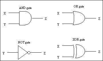
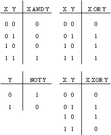
Figure 1 - Basic logic gates and their truth tables
Each gate’s operation is described by a truth table, which basically provides the same information as a verbal description.
Digital Logic Analysis
We can build more complicated circuits by connecting different gates together in a way such that the circuit performs the desired purpose. This is generally called circuit design. Going in the reverse direction, (i.e. breaking a pre-existing circuit down into its logic gates and then writing equations on the arrangement) is the essence of circuit analysis. The best way to demonstrate circuit design is by example. Usually you begin with the inputs and write down the logic expression at the output of each gate as you proceed toward the final output (or outputs.) The ordering doesn’t matter, unless one of the inputs you’re working on comes from an output of a previous logic gate. Below, we see an example of an arbitrary circuit using some of the earlier defined logic gates. We could start with the inverter gate and write logic expression of this logic gate (which in this case is to invert the incoming signal A to A’), on the line to the right of the gate. We then take the A’ and the signal B as inputs to the AND gate and write the operation of this logic gate on the line to the right as shown. You’ll usually end up with some complicated-looking expressions for the final outputs (in this case there is only one output, Z.)
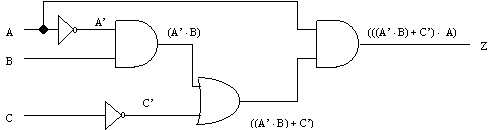
We want to analyze the behavior of this circuit to see what combination of inputs will cause the output to "go high" or become 1. To do this we write a truth table with the inputs in the leftmost columns. Each expression that we wrote on the circuit can be written as a "step" at the top of each column, with the final equation in the rightmost column. Below the inputs, we write all possible binary combinations of those inputs. Below the expression in each column we write the binary output of each gate (i.e. the result of each expression.) An example of a truth table for the above circuit is shown below.
A |
B |
C |
A’ |
(A’ + B) |
C’ |
((A’ × B) + C’) |
Z = (((A’ × B) + C’) × A) |
0 |
0 |
0 |
1 |
0 |
1 |
1 |
0 |
0 |
0 |
1 |
1 |
0 |
0 |
0 |
0 |
0 |
1 |
0 |
1 |
1 |
1 |
1 |
0 |
0 |
1 |
1 |
1 |
1 |
0 |
1 |
0 |
1 |
0 |
0 |
0 |
0 |
1 |
1 |
1 |
1 |
0 |
1 |
0 |
0 |
0 |
0 |
0 |
1 |
1 |
0 |
0 |
0 |
1 |
1 |
1 |
1 |
1 |
1 |
0 |
0 |
0 |
0 |
0 |
With more practice in writing truth tables, it won’t be necessary to write all of the intermediate steps in the columns. Also, notice that this example used signals that were only 1-bit "wide" so to speak. There can be 4, 8, or even 16 parallel multi-bit signals for each line on a diagram. These are usually marked with a diagonal slash on the line with a number above indicating how many actual data lines are being represented by the "line" on the diagram.
C.) Digital Logic Design
The flip-side of this story is design, where we start with the desired behavior of a circuit, and then design the circuit, by connecting different logic gates together, that will satisfy this desired behavior. This begins with viewing the circuit as a black box (see below) that will take the given inputs and will cause the output to be high only for the combinations of the inputs that we want it to.
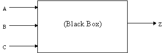
Say, for example that this "black box" circuit needs to satisfy the requirements in the table below (the results from the previous analysis example.)
A |
B |
C |
Z |
0 |
0 |
0 |
0 |
0 |
0 |
1 |
0 |
0 |
1 |
0 |
0 |
0 |
1 |
1 |
0 |
1 |
0 |
0 |
1 |
1 |
0 |
1 |
0 |
1 |
1 |
0 |
1 |
1 |
1 |
1 |
0 |
So, the question is, how do we translate the desired behavior into a Boolean function, so that we can design the circuit? The answer lies in what is called the "Sum-of-Products" formulation. It is based on the concept of "minterms". Look at the truth table. We want the function to be 1 when A is 1, B is 0 and C is 0; and when A is 1, B is 1, and C is 0; and to be 0 for every other combination of values for A, B, and C. Consider the first set (1, 0, 0). A function which is 1 for this choice and 0 else is exactly the function Z4 = A × B’ × C’ (We AND either the variable or its complement based on whether we need it to respond to a 1 or a 0).
*** Write the truth table for Z4 to verify this claim*** This function is called the 4-minterm; "4" because the code (1, 0, 0) can be interpreted as the binary number for 4. For the second place that we want Z to be 1 (1, 1, 0), the correct minterm is Z6 = A × B × C’ (see the pattern?). Since we want z to be 1 for either of these conditions, we write Z = Z4 + Z6 = A × B’ × C’ + A × B × C’. This format is the "Sum-of-Products" or "SOP" for the function Z, given by the above truth table. *** Write out the truth table for the SOP to see that it is exactly the desired truth table. *** This is sometimes written as S A,B,C(4, 6); the 4 and 6 referring to the rows in the truth table where the function is 1.
Once the Boolean function is known, it is quite straightforward to draw the digital circuit. One important point is that Boolean functions are NOT unique. By applying the theorems of Boolean algebra, we can simplify the function (Why? To reduce the number of gates needed to realize the function.) For example:
A × B’ × C’ + A × B × C’ = A × C’ × B’ + A × C’ × B (why?)
= A × C’ × (B’ + B) (why?)
= A × C’ × 1 (why?)
= A × C’ (why?)
which is clearly a much easier circuit to build. There are formal mechanisms to do this circuit minimization that you will learn in the next course. Right now, it’s enough to know how to translate from a description of what the circuit is supposed to do, to a truth table, to the SOP, to a circuit diagram.
As a practical example, consider the problem of adding two bits. This circuit actually has three inputs: two bits, X, Y, and a carry-in, CI. It must produce two outputs: the sum, S, and the carry-out, CO. From our experience, we know now that the circuit must satisfy the following constraints.
CI |
X |
Y |
S |
CO |
0 |
0 |
0 |
0 |
0 |
0 |
0 |
1 |
1 |
0 |
0 |
1 |
0 |
1 |
0 |
0 |
1 |
1 |
0 |
1 |
1 |
0 |
0 |
1 |
0 |
1 |
0 |
1 |
0 |
1 |
1 |
1 |
0 |
0 |
1 |
1 |
1 |
1 |
1 |
1 |
Using the SOP formulation, we see that S = S CI,X,Y(1, 2, 4, 7) and that CO = S CI,X,Y(3, 5, 6, 7). *** Write out that full Boolean functions for S and CO, draw the circuits using Inverters and only 2-input AND’s and OR’s, and use Boolean Algebra to simplify the functions. ***