Computer
Engineering / Computer Science 126

Supplemental Notes
Dr. Jim Keller, Dr. Michael Jurczyk, and Jerry Moore[Chapter 1] [Chapter 2] [Chapter 3] [Chapter 4]
Sequential Logic Analysis
A.) Introduction and Motivation
Combinational logic circuits only depend on what the input values are now. Sequential circuits not only depend on the current values of the inputs, but they also depend on what those inputs were in the past. While combinational logic is great for controlling devices, it doesn’t provide a way to temporarily store any information. The outputs are immediately changed as soon as signals that carry the changes in the inputs reach them, with no memory of what the previous sequences of inputs were. In other words, a combinational logic circuit is not regulated by time because it is not involved with a clocking device, and it doesn’t remember anything from the past because it doesn’t contain any memory elements.
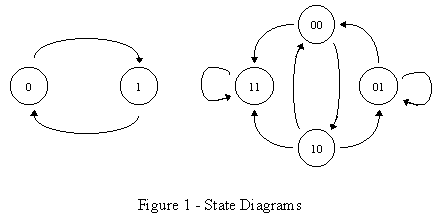
These two elements, the clock and the basic memory element, give the sequential circuits a significant advantage: the capability of remembering states. A state is just a collection of state variables. Each state variable can be represented by a bit. Therefore n bits, or state variables, can produce 2n different states. In Figure 1 there are two examples of sequences of states. The state diagram on the left is composed of only two states (since there can only be two possible combinations of one bit - 0 and 1.) The diagram on the right has two bits representing 4 possible states (22 = 4.) If the diagram on the right were a simplified state diagram of an ATM machine, state 00 could be receiving the user’s ATM card, state 01 could be prompting the user for their desired transaction, state 10 could be recording and executing the user’s desired transaction, and state 11 could be returning the user’s ATM card, receipt, and cash (if it was a withdraw.) The state diagrams presented here are only to introduce you to the idea that a machine can be in different states as it processes data. But before we go further, we must look into how a circuit can store information.
B.) R-S Latch
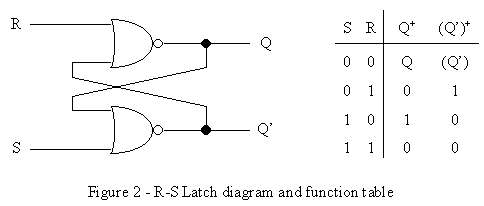
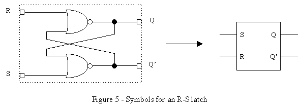
This raises the question: how can we build a circuit to store just one bit of information? Once we accomplish this, we can just duplicate this circuit to build storage units to hold information of any size. We begin by introducing the R-S latch, which is the basic building block for memory. This circuit (see Figure 2) uses two NOR gates in a feedback configuration (although you can also use two NAND gates with some slightly different results), to effectively store one bit of information. The value of Q is the current stored output value for this latch circuit, and remembering our previous discussion about states, Q would be called a state variable. This circuit is sometimes incorrectly given the nickname "flip-flop", because the values of Q and Q’ are traditionally opposite with each other (i.e. if Q is 1, then Q’ must be 0), and so they will sometimes flip when the inputs are certain values. (We will later see one exception to this rule with the R-S latch.) The R stands for reset, and when asserted to a 1 (with S remaining 0), it causes Q to become 0 and Q’ to become 1, which effectively clears the latch (see the function table.) The S stands for set, and when asserted to a 1 (with R remaining 0), it causes Q to become 1 and Q’ to become 0, which effectively presets the latch. As you can also see from the table, if R and S are both left at 0, then the latch will "remember" its previous value and not change. This is indicated by the plus signs on the Q’s, where Q indicates the current value of the state variable Q, and Q+ indicates the new (or next) value. If R and S are both asserted to 1, then both Q and Q’ are forced to 0, which is one undesirable attribute of the R-S Latch that we mentioned earlier.
The function table describes the basic behavior of this R-S latch circuit, but to see the actual dynamic behavior, we need to look at a timing diagram of an R-S latch. This diagram shows the internal behavior of the circuit when different input sequences are applied to the circuit. To understand the timing diagram, we first need a little explanation of the dynamic behavior of the logic gates. The time it takes a signal to propagate from an input of a logic gate to the output is called the propagation delay. If you haven’t any prior experience with digital logic, you’ll learn in later courses that propagation delay, along with many other specifications must be found from formulas or looked up in data manuals like the TTL Data Book by Texas Instruments. For the purposes of this class, we will simplify matters by only worrying about the propagation delay, which will be given as part of the problem. For example, in Figure 3 we are given an R-S latch with a propagation delay of 10ns (nanoseconds or 1 x 10⁻⁹s) per logic gate.
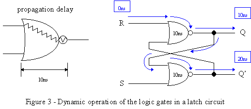
A signal change at R takes 10ns to propagate through the upper logic gate and reach Q. It then feeds back into the lower logic gate instantaneously, and then takes another 10ns (a total of 20ns since the signal change at R) to propagate through the lower logic gate and reach Q’. A similar reaction occurs if there is a signal change at S, except Q’ is changed after 10ns and Q is changed after 20ns. Two examples of timing diagrams of the above circuit are shown in Figure 4. Notice that the 10ns propagation delay on the gates in Figure 3 corresponds with the 10ns delay between the vertical lines in Figure 4. In other words, since all other signal propagation in our simplified model is assumed to happen instantaneously, the only delay that affects the time between the "ticks" in the diagram is the propagation delay. The horizontal lines drawn above the dotted line are assumed to have the value 1 and those below the dotted line are 0. Notice on the left diagram that, depending on the circumstances, a change in R will be seen by Q first, and then by Q’ second, and a change in S will be seen by Q’ first and then by Q second. Timing diagrams can be quite tricky with more complicated input signals. Notice on the left diagram at t3, that the Q’ signal is NOT rising at the same time with S because it is responding to S, for this is impossible because there must be a 10ns delay between S and Q’. It is rising because it is responding 20ns after R changed and 10ns after Q changed, exactly the way it should be.
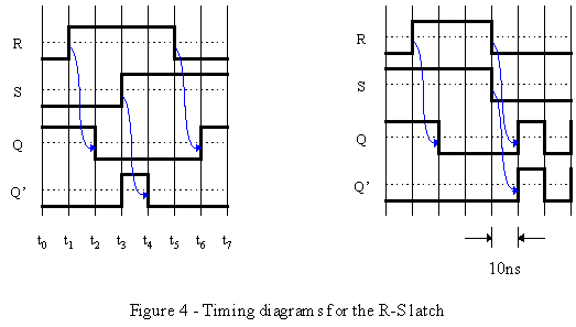
Recall that the first undesirable attribute of the R-S latch is the illegal state that can be produced when Q and Q’ both go to zero. In Figure 4 on the right we see the second property of the R-S flip-flop that makes it very unpopular. If both the R and S inputs go from being asserted to unasserted at the same time, the flip flop becomes unstable and the Q and Q’ outputs oscillate unpredictably. To show this, we draw the outputs as following each other instead of being opposite of one another. This undesirable property of the R-S latch led to the design of other types of circuits that we will see shortly. *** It would be a very good idea to work out these two examples on your own and verify these results. ***
Now that we’ve discussed the internal behavior of the R-S latch circuit, we can represent it with a box that represents a single bit of memory storage (see Figure 5.) Whether the S and R match the Q and Q’ doesn’t matter since its external behavior is determined from the function table back in Figure 2.
C.) R-S Latch with Enable
The first element that gave sequential circuits a significant advantage was the basic memory storage. The second element is usage of the clock to control when changes in the inputs are felt in the logic circuits. The simplest way to incorporate the clock into a latch circuit is to AND each input signal with an enable signal that is somehow linked to or timed by the clock
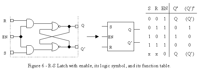
(see Figure 6.) Therefore, changes in the inputs are seen by the latch circuit only when the enable is high. While having the enable gives us the added convenience of being able to activate or deactivate the latch circuit, it does nothing to solve the two undesirable qualities of the R-S Latch.
D.) R-S Flip-Flops
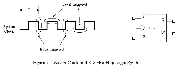
On a timing diagram, the clock is usually represented as a square wave having a specified period T(see Figure 7.) We won’t be concerned with the details of clocked circuits at this level. We only need to know that there are two basic kinds of clocked devices: level-triggered and edge-triggered. With level-triggered devices, the inputs affect the circuit when the clock is either high or low, but with edge-triggered devices, the inputs affect the circuit when the clock is making its transition from low to high, or from high to low. You can think of an R-S Latch as a level-triggered device with its enable always connected to a "high" signal. Because this R-S Latch is always enabled, it watches its inputs continuously and can change its outputs at any time. This is the distinguishing characteristic between a latch and a flip-flop. The R-S Flip-Flop normally samples its inputs and changes its outputs only at times determined by the clocking signal.
The R-S Flip-Flop also corrects one of the two undesirable properties of the R-S Latch. The flip-flop only samples its inputs and changes its outputs during a small interval within each clock period. Once this interval is over, the values of the inputs are ignored and those of the outputs are "locked" into place until the next interval is reached. Obviously this requires the circuitry to be a little more complicated, but we are only concerned with how the flip-flop functions. From now on, we will deal primarily with flip-flop circuits. In addition, all of our memory devices will have a dynamic input indicator (the small triangle) to indicate that they are edge-triggered, but we won’t deal with the clock as an input, we’ll just recognize that it is needed for the circuit to function. In place of the enable (EN) we’ll use the clock (CLK) signal.
E.) D Flip-Flops
The D flip-flop can be built from the R-S flip-flop with just a simple inverter (see Figure 8.) This eliminates the second undesirable property of the S-R Latch by removing the illegal state. Both the S and R inputs can no longer assume the same value at the same time and possibly cause the outputs to equal one another. The inverter forces the inputs to assume opposite values.
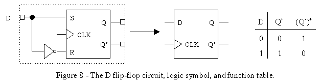
As you can see from its function table, the D flip-flop output, Q, follows the input signal. This flip-flop is popular for constructing 8 or 16-bit registers and other more complicated devices you will later learn about.
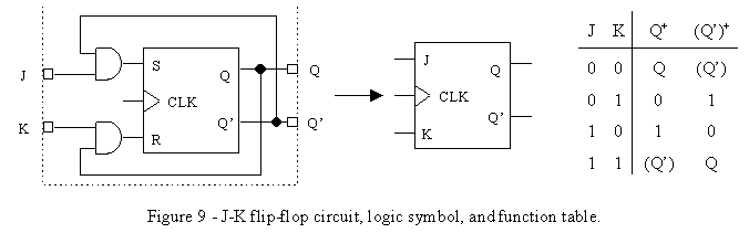
F.) J-K Flip-Flops
There are several different ways to construct J-K flip-flops using devices that we already know. The first way is to use an edge-triggered R-S flip-flop like in Figure 9. The operation of this circuit is identical to an R-S flip-flop, substituting J for S and K for R, except when both J and K are simultaneously asserted, the output Q "flips" to whatever the current state of Q’ was, and Q’ "flips" to whatever the current state of Q was. In effect, they swap values.
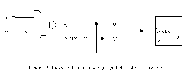
A second design uses an edge-triggered D flip-flop instead, with an added OR gate (see Figure 10.) The functionally of both of them are equivalent.
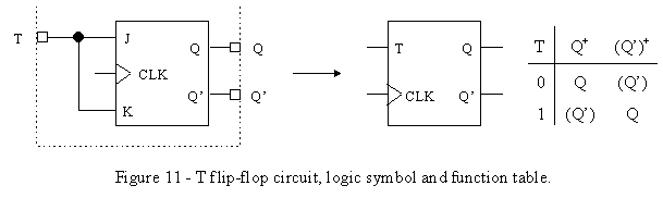
G.) T Flip-Flops
The output of a T flip-flop only changes when the value of the input is a 1. When this happens, Q and Q’ swap values (or "toggles"), similar to the J-K flip-flop when both J and K equal 1. Notice that if the input is periodic, the output Q of the T flip-flop circuit has exactly half the frequency of the input signal. This makes the T flip-flop useful in oscillation circuitry, where for example, a computer clock frequency must be cut in half or smaller. When several T flip-flops are connected together, they can also be used as counters.
H.) Sequential Circuit Analysis
Now that we have the tools required to understand the operation of these basic memory devices, we can combine them together into a larger sequential circuit and predict how the circuit behaves. Recall the earlier discussion about how machines and circuits can operate in a series of steps or states. How these states are organized and what the corresponding values for the outputs are depends on the design of the sequential circuit. All sequential circuits have what is called state memory, which is where the flip-flops store the current state of the circuit, and two combinational "sub-circuits" that perform two totally different functions (see Figure 12.) The first circuit determines what the outputs will be for the current state, and is called the output
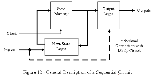
logic. The second circuit takes the current state and the inputs and determines what the next state will be; it is called the next-state logic. Notice that only the state memory is involved with the clock, the rest of the logic is purely combinational. There are two general types of sequential circuits: Mealy machines and Moore machines. The outputs of the Moore machine can only change with the clocking signal, and therefore does not include the dotted connection in Figure 12. The Mealy machine, however, can change its outputs with the clock, or when one or more of its inputs change.
The best way to explain this process is to work through an example. In Figure 13 we have an example of a Moore-type sequential circuit using T flip-flops. (One could easily make this a Mealy circuit by connecting the X input into the NOR gate near the Y output.) This circuit may look confusing at first, but if we break its analysis down into parts, we can easily find the information that will enable us to predict its behavior. Notice that the NOR gate corresponds to the output logic, and that the two AND gates along with the OR gate make up the next-state logic. The two T flip-flops would then be the state memory. The analysis can be divided into 3 main parts: finding the state equations (or excitation equations) and the output equations, writing out the truth table, and drawing the state diagram.
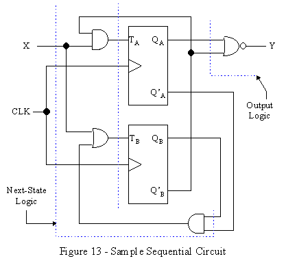
Finding the state equations enables us to know how the combination of inputs and the current state will affect the next state in the circuit. Therefore we must find the equation for every input to each individual flip-flop. For the example in Figure 13, each T flip-flop has only one input: TA for the top one and TB for the bottom. By just looking at the circuit, we can see that the equation for TA is just the opposite of the state variable QB ANDed with the input X. In a similar manner we can find the other state equation for TB and the output equation for Y. The equations are as follows:
![]()
![]()
![]() (using DeMorgan’s
Law)
(using DeMorgan’s
Law)
Once we have the state and output equations, we can immediately begin the state table by writing the inputs first across the top row, then the current state variables (indicated by the minuses), the inputs to the flip-flops, the next state variables (indicated by the pluses), and finally the outputs (see Table 1.) Under the inputs and the current state variables, write all possible binary combinations of these variables. (For our example, we write down 8 rows because for 3 variables, there can only be 23 or 8 possible combinations.) Now we fill in the
Table 1 - Example state table
(Inputs and current states) |
(Inputs to flip-flops) |
(New states) |
(Outputs) |
||||
X |
QA |
QB |
TA |
TB |
Q+A |
Q+B |
Y |
0 |
0 |
0 |
0 |
0 |
0 |
0 |
0 |
0 |
0 |
1 |
0 |
1 |
0 |
0 |
1 |
0 |
1 |
0 |
0 |
0 |
1 |
0 |
0 |
0 |
1 |
1 |
0 |
0 |
1 |
1 |
0 |
1 |
0 |
0 |
1 |
1 |
1 |
1 |
0 |
1 |
0 |
1 |
0 |
1 |
0 |
0 |
1 |
1 |
1 |
0 |
1 |
1 |
0 |
1 |
0 |
1 |
1 |
1 |
0 |
1 |
1 |
0 |
0 |
rows for the inputs to the flip-flops using the state equations and the values for the current state variables and the inputs. (For our example, we start with the first row under TA. The negation of QB is 1 in that row, but the value of X in that row is 0. Since the equation for TA AND’s these together, the result for TA in that spot is 0. The same procedure is used for TB with its own state equation.) Next we must find values for the next state variables in each row. Here’s where the knowledge of the flip-flops comes into use. We know that for a T flip-flop the output Q "toggles" only when the input T is equal to a 1. Note that Q+A is only affected by the TA column, and that Q+B is only affected by the TB column. Looking at row two of Table 1, we see that TA is 0 and TB is 1. Since TA is 0, the current value of the flip-flop will not change, and the new value will remain 0. However TB is 1, so the flip-flop will change state from a 1 to a 0. Once all of the new states have been filled in, we can then finish the state table by filling out the output columns. By using the output equations in the same way as we used the state equations for the inputs to the flip-flops, we can plug in and find the output values. Remember: the output values are based on the current values of the state variables, NOT on the new values.
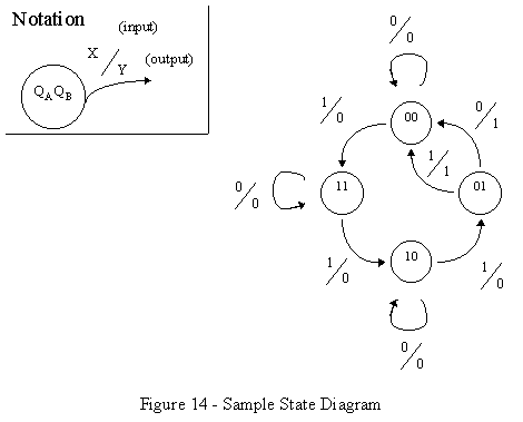
Now that we have this state table, how do we interpret it? When using the state table to draw a state diagram, we are mainly concerned with the old state, the new state, the inputs, and the outputs. If we understand the concepts of sequential circuits, then the meaning of a row in the state table becomes clear. For example, read row 7 of our state table above and you’ll discover it means the following: "If we are currently at the state 10, and the input X equals 1, then the next state will be 01 and the output Y will be 0." If we look at the state diagram in Figure 14, we see that there is a directed line going from state 10 to state 01 that corresponds to row 7 in the state table. From this we see that the number of lines of the state diagram must equal the number of rows in the state table. The value of the input X = 1 is written over a slash near the directed line, while the output Y = 0 is written under the slash. Note that there are only four states because there are only two memory elements (T flip-flops) each storing only a single bit. Remember that n bits can have 2n possible combinations, with each combination representing a state (22 = 4 states.) Not all combinations have to be used however. The columns containing inputs to the flip-flops (TA and TB in our example) are only used to help find the values for the next state, and are usually ignored when drawing the state diagram. *** It would be a good idea to verify these results on you own! *** Remember that you can have any number of inputs and outputs, and that one circuit can contain a mix of different types of flip-flops.